Product Summary
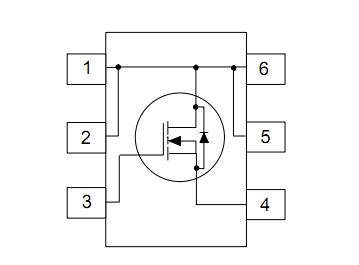
The FDC653N is an N-Channel enhancement mode power field effect transistor. It is produced using Fairchild’s proprietary, high cell density, DMOS technology. This very high density process is tailored to minimize on-state resistance. The FDC653N is particularly suited for low voltage applications in notebook computers, portable phones, PCMICA cards, and other battery powered circuits where fast switching, and low in-line power loss are needed in a very small outline surface mount package.
Parametrics
FDC653N absolute maximum ratings: (1)VDSS Drain-Source Voltage: 30 V; (2)VGSS Gate-Source Voltage: ±20 V; (3)ID Drain Current: 5 A; (4)PD Maximum Power Dissipation: 1.6 W; (5)TJ,TSTG Operating and Storage Temperature Range: -55 to 150℃.
Features
FDC653N features: (1)5 A, 30 V. RDS(ON)= 0.035Ω @ VGS = 10 V; RDS(ON) = 0.055Ω @ VGS = 4.5 V; (2)Proprietary SuperSOTTM-6 package design using copper lead frame for superior thermal and electrical capabilities; (3)High density cell design for extremely low RDS(ON); (4)Exceptional on-resistance and maximum DC current capability.
Diagrams

| Image | Part No | Mfg | Description |  |
Pricing (USD) |
Quantity | ||||||||||||
|---|---|---|---|---|---|---|---|---|---|---|---|---|---|---|---|---|---|---|
 |
 FDC653N |
 Fairchild Semiconductor |
 MOSFET SSOT-6 N-CH 30V |
 Data Sheet |

|
|
||||||||||||
 |
 FDC653N_F095 |
 Fairchild Semiconductor |
 MOSFET 30V 5A N-CH ENHANCEMENT MODE |
 Data Sheet |
 Negotiable |
|
||||||||||||
 (China (Mainland))


