(China (Mainland))

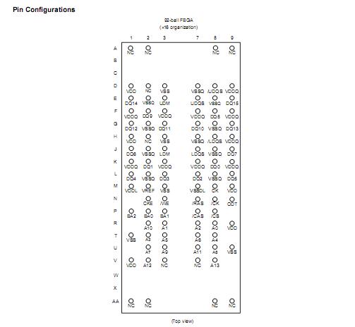
Product Summary
The EDE2116ABSE-8G-E is a 2G bits DDR2 SARAM. The EDE2116ABSE-8G-E must be powered up and initialized in a predefined manner. The EDE2116ABSE-8G-E should be in all bank precharge with CKE already high prior to writing into the mode register.
Parametrics
EDE2116ABSE-8G-E absolute maximum ratings: (1) Power supply voltage VDD: -1.0 to +2.3V; (2) Power supply voltage for output VDDQ: -0.5 to +2.3V; (3) Input voltage VIN: -0.5 to +2.3V; (4) Output voltage VOUT: -0.5 to +2.3V; (5) Storage temperature Tstg: -55 to +100°C; (6) Power dissipation PD: 1.0W; (7) Short circuit output current OUT: 50mA.
Features
EDE2116ABSE-8G-E features: (1) Double-data-rate architecture; two data transfers per clock cycle; (2) The high-speed data transfer is realized by the 4 bits prefetch pipelined architecture; (3) Bi-directional differential data strobe (DQS and /DQS) is transmitted/received with data for capturing data at the receiver; (4) DQS is edge-aligned with data for READs; center-aligned with data for WRITEs; (5) Commands entered on each positive CK edge; data and data mask referenced to both edges of DQS; (6) Data mask (DM) for write data; (7) Off-Chip-Driver Impedance Adjustment and On-Die-Termination for better signal quality; (8) /DQS can be disabled for single-ended Data Strobe operation.
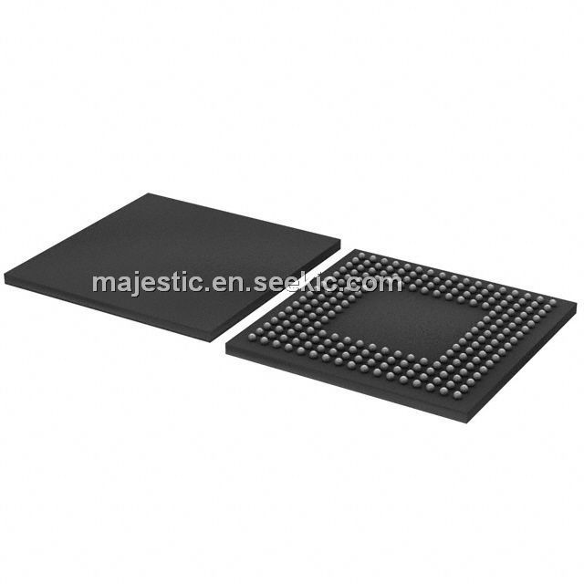
Diagrams